


- Integrated with the EMC laboratory, IKERLAN offers a comprehensive service covering the entire electronic development cycle, strengthening the industrial competitiveness of the region.
The technology centre IKERLAN has inaugurated a new advanced electronics laboratory at its headquarters in Arrasate. This infrastructure will allow industry to significantly shorten product development cycles, from design to final validation.
The main innovation of this facility, unique in Euskadi, is the ability to develop printed circuit boards (PCBs) in-house. Until now, this process was largely outsourced abroad, impacting lead times and increasing dependency in a context marked by supply chain instability. Thanks to this integration, prototyping times can be reduced from several weeks to just a few days.
The laboratory is integrated with the electromagnetic compatibility (EMC) testing lab, enabling the entire electronic product development cycle to be carried out in a single environment: design, prototyping, verification, early problem detection, validation and preparation for industrialisation. “Companies need to develop faster, test variants and adapt their designs within very short timeframes. With this laboratory, we respond to that need by increasing agility and reliability in prototyping”, said Ion Etxeberria, CEO of IKERLAN, during the inauguration event.
This new laboratory strengthens IKERLAN’s position as a leading technology partner for industry, in a context where technological autonomy and supply chain resilience are key.
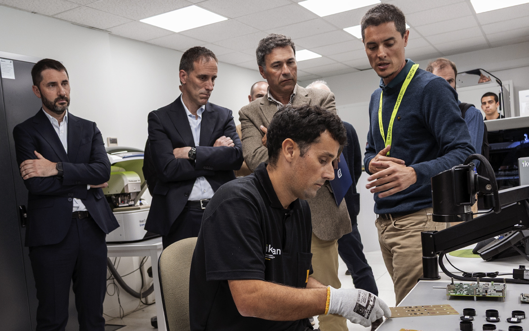
The infrastructure has been supported by the Provincial Council of Gipuzkoa. The inauguration event was attended by Unai Andueza, Deputy for Economic Promotion; Jon Gurrutxaga, director of innovation of the provincial council; Ion Etxeberria; Jon Pérez, Director of Embedded Electronic Systems and Cybersecurity at IKERLAN; Pello Rodríguez, President of MONDRAGON and representatives from several companies interested in learning first-hand about the facility.
During the visit, Andueza highlighted that this infrastructure “contributes to accelerating innovation and strengthening the competitiveness of Gipuzkoa’s industrial fabric, while serving as a clear example of public-private collaboration focused on innovation”.

Key features of IKERLAN’s PCB laboratory
One of the laboratory’s distinguishing features is its ability to develop in-house PCBs of up to 8 layers, incorporating laser-based processes that enable high-density interconnection (HDI) solutions—capabilities that are not widely available in the surrounding industrial environment.
The laboratory is equipped with advanced systems to automate key electronic assembly processes, including high-precision placement systems capable of positioning thousands of components within minutes, as well as soldering technologies that ensure the quality and reliability of prototypes. These capabilities significantly accelerate development times and enhance the robustness of prototyping, particularly in advanced electronics applications.
“We have moved from slow, manual processes to a technological environment that accelerates development and allows us to deliver far more reliable prototypes in drastically reduced timeframes”, said Jon Pérez.

Versatility, security and research
Beyond the agility and versatility it offers to industry, this new infrastructure also strengthens IKERLAN’s research capabilities. It facilitates experimentation with new electronic architectures and their application in fields such as power electronics, embedded systems and embedded artificial intelligence.
It also opens up new opportunities in hardware cybersecurity, enabling the analysis and reinforcement of electronic device security in critical environments.
This laboratory complements other state-of-the-art infrastructures at the centre—such as Digilab, Energylab and Mech Lab—helping to build a comprehensive technological ecosystem that reinforces IKERLAN’s position as a key technology partner for industry.
Integrated with the EMC laboratory, IKERLAN offers a comprehensive service covering the entire electronic development cycle, strengthening the industrial competitiveness of the region.